
Lead
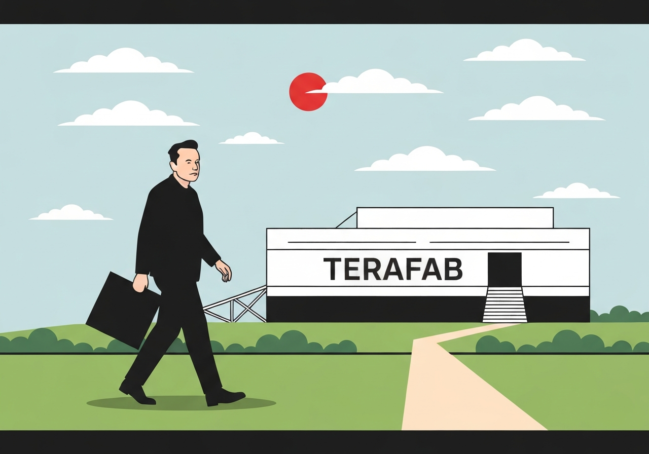
— Elon Musk announced that his Terafab initiative, an ambitious plan to build facilities for designing and producing chips for robotics, AI and space data centers, will begin in Austin and be jointly operated by Tesla and SpaceX. Musk said the project will open with an “advanced technology fab” equipped to fabricate and test a wide range of chips. He reiterated earlier comments that the effort will start at a smaller scale before scaling up to a larger factory. The announcement frames Terafab as a vertically integrated effort spanning Musk’s companies, including xAI, though operational details remain limited.
Key Takeaways
- Announcement date: March 22, 2026; location: Austin, Texas; project name: Terafab, announced by Elon Musk.
- Management: Musk said Tesla and SpaceX will jointly run the initial facility, with xAI referenced as part of the broader program.
- Initial scope: an “advanced technology fab” in Austin that will be outfitted to make and test chips of various types.
- Phasing: Musk reiterated a two-stage approach — beginning with a smaller-scale fab, then expanding to a larger plant.
- Capability claims: Musk described equipment to “make chips of any kind,” a broad claim that would require extensive process expertise and capital.
- Expert caution: Musk has no public track record in semiconductor manufacturing, and his timelines have previously shifted; industry observers note execution risk.
- Strategic rationale: Terafab is positioned to support robotics, AI model training/inference, and SpaceX data-center needs, potentially reducing supply-chain reliance.
Background
Semiconductor fabrication is capital-, talent- and time-intensive. Leading foundries such as TSMC and Samsung deploy billions of dollars and decades of process development to produce advanced chips. Musk’s announcement lands against a global context of strategic interest in onshore chip production and rising demand for specialized AI and robotics accelerators.
Elon Musk oversees multiple ventures — Tesla (electric vehicles and robotics), SpaceX (space launch and satellite systems) and xAI (artificial intelligence). Over recent years he has pushed to vertically integrate components of his technology stack, from vehicle batteries to starlink hardware, arguing that control over critical supply chains improves resilience and performance. Terafab appears to be an extension of that strategy into semiconductors.
Main Event
On March 22, 2026, Musk publicly designated Austin as the site for the initial Terafab facility and described it as an “advanced technology fab” with the tooling to design, fabricate and test diverse chip types. According to his statement, Tesla and SpaceX will operate the site jointly, with xAI named as a program stakeholder. He framed the plan as phased: starting smaller, validating processes, then scaling to a larger manufacturing campus.
Details released so far are high-level. Musk said the Austin fab will contain the equipment necessary to produce and evaluate chips across multiple process nodes, but he did not disclose planned wafer capacity, target nodes (nm), capital expenditure, workforce size or concrete timelines for ramping production. Those operational metrics are critical to assessing feasibility and were not included in the announcement.
The announcement echoes prior remarks from Musk about moving from pilot fabs to larger-scale production. Industry contacts and prior history show Musk has previously set ambitious schedules that were later revised; as a result, many observers are treating the timeline and the claim of universal chip capability as aspirational until technical and regulatory details are published.
Analysis & Implications
If realized, Terafab would represent a notable vertical expansion for Musk’s companies, potentially reducing dependence on external foundries for specialized AI and space-related processors. For Tesla, in-house chip capability could accelerate robotics and vehicle autonomy hardware cycles. For SpaceX, closer control of space-data-center silicon could improve latency, radiation-hardening customization and integration with satellite systems.
However, fabrication mastery requires decades of accumulated process knowledge, supply-chain relationships, and high-volume production economics. Established foundries achieve cost efficiencies through massive wafer volumes and process node specialization; a new entrant must either target niche products where volumes are smaller or commit very large capital investment and time to compete on mainstream nodes. That gulf presents both business risk and technical hurdles for Terafab.
Geopolitically, locating the project in Austin aligns with broader U.S. interest in domesticizing chip manufacturing and securing supply chains for critical technologies. Politically and financially, the project could attract state and federal incentives, but it will also face scrutiny over subsidies, workforce training needs and environmental permitting for fab operations.
Comparison & Data
| Item | Announced Terafab (Musk) | Typical Leading Foundry |
|---|---|---|
| Location | Austin, Texas | Multiple global sites (Taiwan, S. Korea, US) |
| Scale at announcement | Pilot/advanced fab, phased expansion | Large-scale wafer fabs with >50k wafer starts/month |
| Public timeline | Initial small fab then larger | Multi-year development and ramp |
The table highlights the information gap: Musk has confirmed Austin and a phased approach but has not provided capacity, node targets or funding details. Those variables determine whether Terafab will be a niche pilot facility or evolve into a major commercial foundry.
Reactions & Quotes
Below are direct excerpts and contextual reactions tied to the announcement.
“An advanced technology fab”
Elon Musk (announcement)
That phrase was Musk’s shorthand for a facility he said would include tooling to make and test varied chip types; the company has not released a detailed equipment list.
“Starting small, then scaling up is sensible in principle, but execution is the hard part.”
Industry analyst (trade commentary)
Analysts emphasize that pilot fabs can validate processes, but scaling to competitive yields and volumes commonly proves the most difficult phase.
“A domestic fabs push aligns with national priorities for chip resilience.”
Policy observer (technology policy)
Policy specialists note the announcement could accelerate state and federal engagement on incentives, workforce development and permitting decisions in Texas.
Unconfirmed
- Exact wafer capacity, node targets (nm) and annual output have not been disclosed by Musk or the companies and remain unconfirmed.
- Specific operational roles for xAI in design, fabrication or testing are not detailed and require confirmation.
- Planned timeline for moving from the initial small fab to a larger campus, including funding sources and permits, has not been published.
Bottom Line
Elon Musk’s announcement that Terafab will begin in Austin under joint Tesla and SpaceX supervision marks a high-profile move into semiconductor manufacturing for his ecosystem of companies. The plan promises in-house capability for chips serving robotics, AI and space systems, aligning with broader industry and policy trends toward domestic fabrication.
Practical execution, however, faces steep technical and economic barriers. Key questions—production capacity, node targets, capital commitments and workforce plans—remain unanswered. Observers should treat the Austin declaration as an important strategic intent but await detailed engineering, financial and regulatory filings before concluding on Terafab’s likely scale or market impact.
Sources
- Bloomberg — News report summarizing Musk’s March 22, 2026 announcement (news)