
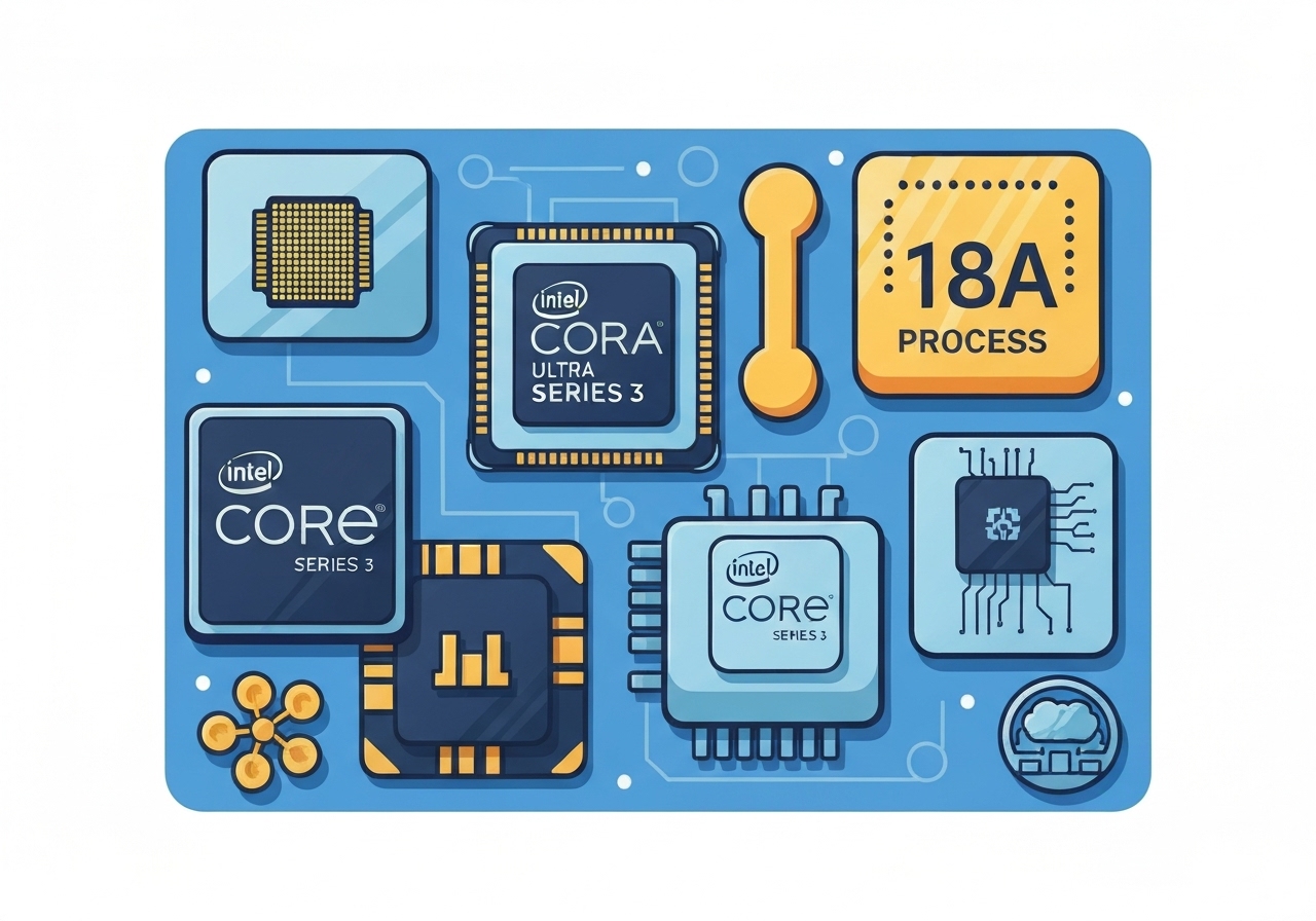
Intel this month rolled out its Core Ultra Series 3 (Panther Lake) processors, marking the first consumer chips built on the company’s long-awaited 18A node. The new parts use a chiplet design joined via Intel’s Foveros packaging: the compute tile that holds CPU cores and the NPU is the 18A die. Intel presented three primary configurations and performance claims that include up to 60 percent faster multi-core CPU throughput and up to 77 percent faster integrated GPU performance versus the prior Core Ultra 200V family. The launch also included a Lenovo IdeaPad reference result that reported 27.1 hours of 1080p Netflix streaming on a Core Ultra X9 388H test unit.
Key Takeaways
- Intel’s compute tile for Panther Lake is produced on the 18A process and ships in two variants: one with up to 16 CPU cores and another with up to 8 CPU cores.
- The platform controller tile and the high-end 12-core graphics tile are manufactured at TSMC; the simpler 4-core graphics tile is built on Intel 3.
- Chiplet combinations yield three headline SKUs: 16-core CPU with 12-core GPU, 16-core CPU with 4-core GPU, and 8-core CPU with 4-core GPU, with additional stepped-down parts achieved by disabling cores.
- Intel claims up to 60% faster multi-core CPU performance and up to 77% faster integrated GPU performance compared with Core Ultra 200V chips.
- All Panther Lake chips include the same NPU delivering up to 50 TOPS, surpassing Microsoft’s 40 TOPS Copilot+ threshold but below AMD’s 60 TOPS and Qualcomm’s 80 TOPS claims.
- Connectivity highlights include Wi‑Fi 7, Bluetooth 6.0, and up to four Thunderbolt 4 ports on supported designs.
- Intel presented a Lenovo IdeaPad reference design with a Core Ultra X9 388H that streamed Netflix at 1080p for 27.1 hours in a lab test; real-world battery life will vary by system configuration and settings.
Background
Intel’s move to a chiplet strategy and advanced packaging reflects a broader industry trend away from monolithic dies toward heterogeneous tiles optimized on different nodes. Foveros stacking and tiled packaging let Intel mix compute, GPU and I/O tiles produced at different fabs and process generations into a single package, easing yield and scheduling constraints. The 18A node has been framed internally as a milestone for Intel’s roadmap because it signals progress on the company’s most advanced manufacturing targets after several public delays over recent years. Externally, the launch is framed as part of Intel’s IDM 2.0-era push to combine internal fabs with external foundry relationships to accelerate product cadence and scale production.
Panther Lake arrives in a competitive landscape where AMD, Qualcomm and others stress AI performance and energy efficiency as key battlegrounds. Microsoft’s Copilot+ PC initiative has created a baseline requirement (40 TOPS) for on-device AI performance, and vendors are using TOPS figures as a shorthand to compare NPUs. Intel’s 50 TOPS claim positions its NPU comfortably above that baseline, though competitors are advertising higher peak TOPS numbers. Beyond raw chips, OEM partners and reference designs will determine how the new SoCs translate into end-user battery life, thermals and feature sets across laptops and mobile platforms.
Main Event
At the heart of the announcement is the compute tile, the only tile fabricated on Intel 18A and housing the CPU cores plus the neural processing unit. Intel revealed two compute-tile configurations: one capped at 16 CPU cores and another capped at 8. The company pairs these tiles with different graphics and platform-controller tiles to produce multiple SKUs without reworking the compute die.
The platform controller tile, which consolidates most I/O functions, continues to be produced by TSMC, as does the high-end 12-core graphics tile used in Intel’s top configuration. To reduce complexity for lower tiers, Intel uses a four-core graphics tile built on Intel 3, a process previously applied to some Xeon server dies. That mixing of foundries and process nodes is presented as a practical compromise to bring 18A compute capacity online while balancing cost and yield.
Intel laid out three main Panther Lake combinations and said additional SKUs are produced by disabling CPU or GPU cores as needed. For marketing and benchmarks, the company highlighted broad performance uplifts versus the prior Core Ultra 200V generation: up to 60 percent in multi-core CPU workloads and up to 77 percent in integrated GPU scenarios. Intel also emphasized connectivity and system-level features—Wi‑Fi 7, Bluetooth 6.0 and multiple Thunderbolt 4 ports—targeting premium laptop designs.
Analysis & Implications
Technically, shipping a consumer compute tile on 18A is a symbolic and practical accomplishment for Intel: it indicates the most advanced Intel node is producing usable silicon and that Intel can integrate it with tiles made elsewhere. That hybrid-sourcing approach reduces the pressure on any single fab and enables a rapid product mix, but it also means Intel’s final performance and availability will depend on partner supply and cross-fab coordination.
From a competitive standpoint, Intel’s NPU claim of 50 TOPS is notable because it exceeds Microsoft’s Copilot+ threshold, which could help OEMs market AI-capable laptops. However, AMD and Qualcomm have advertised larger TOPS figures—AMD at 60 TOPS for Ryzen AI 400 and Qualcomm at 80 TOPS for Snapdragon X2—so Intel will need to demonstrate system-level efficiency and software integration to translate raw TOPS into user-visible benefits.
Performance percentage claims (60% CPU, 77% GPU) are significant but should be read in context: benchmark selection, thermals, power limits and system configurations heavily influence results. Intel’s reference battery test (27.1 hours streaming on a Lenovo IdeaPad design) is useful as an illustration of potential endurance but not a substitute for independent reviews across a range of devices and workloads. Market reaction will hinge on real-world performance, OEM design choices, and availability at scale.
Comparison & Data
| Metric | Intel Panther Lake | AMD Ryzen AI 400 | Qualcomm Snapdragon X2 |
|---|---|---|---|
| NPU peak TOPS | 50 | 60 (claimed) | 80 (claimed) |
| Headline CPU cores | up to 16 | varies by SKU | mobile-optimized cores |
| Headline iGPU cores | 12 or 4 | integrated/varies | integrated/varies |
The table summarizes advertised peak NPU TOPS alongside the new Intel core and GPU counts to provide a concise comparison. These figures are vendor claims and do not account for sustained throughput under thermally constrained laptop designs. Benchmarks, power envelopes, and software optimization will determine how these numbers map to user experiences in AI workloads, gaming, and battery-limited tasks. Intel’s mix-and-match tile approach provides flexibility, but it also makes cross-vendor apples-to-apples comparisons more complex unless platform power and thermal targets are standardized.
Reactions & Quotes
Industry and product teams framed the launch as both a technology milestone and a practical step toward broader IDM 2.0 goals.
“Up to 60 percent faster multi-core CPU performance and up to 77 percent faster integrated GPU performance compared to the previous generation,”
Intel (as reported by Ars Technica)
Intel used these comparative percentages to highlight generational gains; however, the company did not publish a full suite of independent third-party benchmark results at the announcement. Observers noted that such percentage claims often derive from selected workloads run under idealized conditions.
“All Panther Lake chips include an NPU capable of up to 50 trillion operations per second,”
Intel (as reported by Ars Technica)
This NPU specification was positioned to meet and exceed Microsoft’s Copilot+ 40 TOPS threshold. Analysts cautioned that TOPS is only one dimension of AI capability and that software stacks, drivers and memory bandwidth are critical to realized performance.
Explainer / Glossary
Unconfirmed
- The long-term production yields and volume capacity of Intel’s 18A fabs for broad consumer supply remain to be independently verified beyond initial shipments.
- The 27.1-hour Netflix streaming figure is a vendor-supplied reference result on a Lenovo design; widespread real-world battery life across OEM models is not yet confirmed.
Bottom Line
Intel’s Core Ultra Series 3 rollout represents a tangible step in the company’s roadmap: the first consumer compute tile on 18A signals progress on advanced process delivery and shows how heterogeneous packaging can mix dies from different foundries. The new chips combine notable uplifts in advertised CPU and GPU throughput with a 50 TOPS NPU that meets current Copilot+ requirements, positioning Intel competitively for AI-capable laptops.
That said, vendor claims should be validated by independent benchmarks and broad OEM product testing. Key near-term indicators to watch are device-level battery and thermal behavior, supply availability for high-end SKUs, and how well software ecosystems leverage the NPU for real-world features. If Intel sustains 18A production and OEMs ship well-balanced designs, Panther Lake could be more than a one-off milestone; if not, it may be a temporary edge in an aggressively contested market.
Sources
- Ars Technica (technology news; reporting on Intel’s launch and claims)